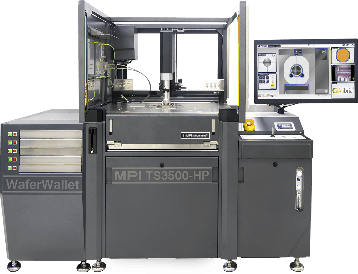
Revealing The Potency Of Advanced Probe Systems
In the challenging realm of semiconductor testing and engineering, only the most cutting-edge systems can truly fulfill the requirements of this dynamic field. We are delighted to present our innovative, powerful probe systems. In this comprehensive overview, we'll explore the noteworthy attributes that make our solutions not just skilled, but indeed unrivaled in the semiconductor analysis domain.
The Advancement of High-Capacity Probe Systems
High-capacity probe systems have seen significant development, fueled by the ever more intricate demands from fields like car manufacturing, power device production, and RF communication. Our high-capacity probe systems are expertly constructed to exceed these emerging requirements, presenting powerful and reliable answers for semiconductor testing.
Utilizing High Power Wafer Probing
At the heart of our advanced systems lies the ability to employ high-energy output in a safe and productive manner. Our unique engineering enables us to manage up to 10kV and 400A, guaranteeing that even the most energy-intensive applications can be addressed with accuracy and reliability. Our systems are specifically designed to prevent electrical discharge and leakage, providing superior security in high power scenarios.
Superior Thermal Management
Heat management plays a crucial role in the sphere of high-throughput testing systems. Our trailblazing solutions incorporate the most state-of-the-art thermal dissipation techniques, thus mitigating heat-induced ineffective processes or damages. Our unique chuck design moreover ensures that the testing card remains thermally unaffected, thus improving the durability and functionality of our high-throughput probe systems.
Impressive Wafer Probing Accuracy
With high-capacity equipment, we take pride in presenting impressive wafer probing accuracy. Due to our cutting-edge technological attributes, we can assure extraordinary contact resistance stability, which is essential for obtaining accurate and reproducible measurements. These systems ensure optimal alignment with each wafer, consequently enhancing the exactness of each examination and diminishing the likelihood of errors.
The Advantage in RF Testing
RF examinations are known to be notably difficult, but our large-capacity equipment are tailored to outperform in this context. With the ability to offer exact, reproducible measurements at high frequencies, our solutions are essential for radio frequency device tests. Our revolutionary technologies eradicate many common complications associated with radio frequency testing, such as issues regarding signal integrity and parasitic capacitance.
An All-Inclusive Solution
Our high-throughput probe systems are more than sturdy testing solutions. They are all-inclusive systems designed to simplify the whole testing process. From early setup and alignment to data compilation and interpretation, our platforms are designed to be intuitive and effective, reducing downtime and enhancing productivity.
High-Power Probe Systems
We are dedicated to the constant development of our large-capacity testing systems. As we look into the future, we envision a exciting landscape of emerging technologies and applications, including electric vehicles to 5G communication, and we are primed to tackle these challenges with 200mm Probing Systems utmost determination. Our engineers are continuously striving to enhance our equipment, making sure that they remain at the cutting edge of semiconductor testing technology.
In conclusion, our high-capacity testing systems are a declaration of our dedication to excellence in the semiconductor testing sector. They represent the peak of precision, power, and performance, acting as holistic solutions to the complex testing requirements of the semiconductor industry.